Introduction
The following suite of programs are intended to be used with USBDM BDM interfaces.
They provide the ability to program the internal Flash memory of the following Freescale microcontrollers:
- RS08, HCS08, HCS12, S12Z, Coldfire V1, Coldfire V2, Kinetis and a limited range of MC56F800x microcontrollers.
Features
- GUI usage is available for interactive use.
- Command line usage is available for batch files.
- Supports most chips - see list below.
- Trimming of internal target clock to specified frequency (RS08, HCS08 & CFV1).
- Programming of security options to leave the chip unsecured or secured after programming.
- May be used to unsecure chips (by mass erase).
- The code has been written in a modular fashion. It should be straightforward to re-use the flash programming code to create other custom programming utilities.
Command Line
Usage:
FlashProgrammer <options> <BinaryFilename>
If neither of the -program or -verify options are given then all options apart from -target are ignored and a GUI interface is opened.
You may rename the executable to e.g. ARMProgrammer to automatically select ARM target.
- BinaryFilename
The name of the S19 or ELF binary file to program.
- Options (order is not significant).
- -bdm=bdm_name
Serial number of preferred BDM to use.
- -requiredBDM=bdm_name
Serial number of required BDM to use.
- -device=device_name
Target device e.g. MC9S08AW16A, MCF51CN128.
- -erase=erase_option
Selects erase method used (Mass, All, Selective, None).
- -execute
Leave target power on & reset to normal mode at completion.
- -flexNVM=eeprom,partition
FlexNVM parameters (eeprom,partition hex values)
- -masserase
Equivalent to erase=Mass.
- -noerase
Equivalent to erase=None.
- -nvloc=address
Trim non-volatile memory location address (hex).
- -power=dur,rec
Power off duration & recovery times (ms).
- -program
Program and verify flash contents.
- -reset=dur,rel,rec
Reset duration, release & recovery times (ms).
- -security=value
Security value (unsecured, image, smart).
- -securityValue=value
Explicit security value to use (as hex string)
- -speed
Communication speed on some targets (kHz).
- -trim=trim_frequency
Trim internal clock to frequency (in kHz) e.g. 32.7.
- -target=target
Type of target e.g. RS08,HCS08,HCS12,S12Z,CFV1,CFVX,ARM,MC56F
- -useReset
Use reset signal.
- -unsecure
Leave device unsecured after programming.
- -vdd=vdd_value
Supply Vdd to target (3V3 or 5V).
- -verify
Verify flash contents.
The program sets the error code to 0 on success, non-zero otherwise.
The program will use the first BDM located. There is no option to select a BDM.
Examples of usage:
- Programming an image with clock trimming:
FlashProgrammer Image.s19 -vdd=3v3 -device=MC9S08AW16A -trim=243 -secure -program -execute
This will program a MC9S08AW16A with the contents of the file Image.s19 and trim the internal clock to 243kHz. Target Vdd will be 3.3 Volts (if this option applies to the BDM used). The Flash image will be modified so that the device will be secure after programming. After programming the device will be left powered and will be reset into normal mode i.e. will be left running the loaded program.
- Programming the clock trim in an already programmed chip:
FlashProgrammer -device=MC9S08QG8 -vdd=3v3 -trim=35.25 -erase=None -program
This will trim the internal clock of MC9S08QG8 to 35.25kHz without erasing the present flash contents. Target Vdd will be 3.3 Volts (if this option applies to the BDM used).
It is necessary that the clock trim locations in flash are still unprogrammed (0xFF) when using the -trim option. The target cannot be secured after trimming.
- Programming image with custom security value:
FlashProgrammer -device=MKL25Z128M4 -vdd=3v3 -erase=mass -program -security=123456789ABCDEF0FFFFFFFFFEFFFFFF Image.elf
This will program the device with Image.elf and explicitly set the security area to '123456789ABCDEF0FFFFFFFFFEFFFFFF'.
Interactive (GUI)
If the program is started without the -program or -verify options then an interactive dialogue is opened to allow the user to configure the programmer. The other options are ignored.
The dialogue has three tabs.
- The first tab is concerned primarily with USBDM interface selection, communication options and general features.
- The second tab is specific to a particular target device.
- The third tab contains other BDM options that are more advanced or less likely to need modification.
Note that the programmer uses a buffer to store the image to be programmed to the device. Some of the following options will persistently modify this buffer. This means that, for example, if you choose the secure option, program the device and then select the image option then further programming will also result in secured devices.
Tab 1 - USBDM
Select BDM - Allows selection between BDMs when multiple are connected
- BDM Selection drop-down box - This displays the serial numbers of the connected USBDM-BDMs. It is useful if each BDM has a unique serial number as that will allow the automatic re-selection of the same BDM on the next session.
If the BDM does not support the required target then a suitable message replaces the serial number. Communication problems will also cause an informative message.
- Detect button - This may be used to scan for changes in the connected BDMs.
- BDM Description - This is the BDM Description obtained from the BDM firmware.
Target Vdd Control - Enables supply of Target Vdd from the USBDM module
- Off, 3.3V or 5V - Controls voltage supply to target through BDM Vdd connection.
- Cycle target Vdd on reset - This option will cause the BDM to cycle the target power as part of the reset sequence.
- Cycle target Vdd on connection problems - This option will cause the BDM to cycle the target power when it is having trouble connecting to the target.
- Leave target powered on exit - The target Vdd supply will be left on when exiting the debugger.
Connection Control - This varies with target
- Automatically re-connect - The option causes the BDM to continuously update the interface speed to prevent loss of communication in case the target speed changes.
- BDM Clock Select - Some targets provide an alternative BDM clock selection which may be at a lower speed that the default. This can have advantages when connecting to high speed targets (mostly of use in the JB16 version). There may be other requirements before the alternative clock will be used.
Note: it appears that HC12 use the Alt source by default so the Normal option may be of more interest.
- Use RESET signal - RS08, HCS08 and CFV1 targets do not require a reset signal for programming.
However it is sometimes useful to drive the reset signal to reset other circuitry connected to the target. Selecting this option will cause the reset signal to be driven.
- Guess speed if no SYNC - Early HCS12s do not support the SYNC feature which allows the BDM interface speed to be determined. Selecting this option will cause the BDM to attempt to find the communication speed by trial and error. This can take quite a while and may be unreliable. Alternatively, set the target speed in the debugger TBDML menu.
- Monitor PST signal - Some CFVx targets provide a PSTALL or PST0-3 signals that may be used to determine if the target is running or halted. If not enabled or not supported by the BDM then a software method is used. The advantage of the PST signal is that it is more reliable in some cases.
- Connection Speed - This drop-down box allows the communication speed on CFVx, DSC and Kinetis devices to be changed. There are severe limitations on the actual speed of the BDM for the JTAG based devices since a software method is used to generate the waveform.
|
|
Tab 2 - Target
- Flash Image Buffer
The programmer makes use of a Flash Image buffer to contain the information to be programmed to the target device. An image of the target flash contents is created in the buffer by loading hex files. The buffer contents may also be altered by some of the later options (Security & Clock trim options modify particular locations immediately before programming).
- Load Hex File
Displays a dialogue to load a Freescale S-format hex file to be programmed to the device. The image buffer is usually cleared before loading the file.
The name of the last/currently loaded file is displayed.
- Linear Image (HCS12 only) This will convert a motorola file from linear address to paged addresses when loading. The programmer uses paged addresses internally. Most motorola files also use paged addresses.
- Incremental file load
Selecting this option prevents the programmer from clearing the buffer before the load of a hex file. This option may be used to assemble a number of hex files into a single image to program to the device. If the contents of multiple hex file overlap then only the last loaded file's values will be programmed. No warning of overlap is given.
- Auto Reload
Selecting this option causes the programmer to automatically reload the last loaded file if its modification date has changed since it was loaded. It does so without a prompt. If this option is not selected then you will prompted to reload each time.
- Device Selection
- Device selection
The drop down box allows the selection of the device type of the chip to be programmed. Selecting a device type will cause most of the dialogue to be automatically completed.
- Detect Chip
This causes the programmer to read the System Device Identification Register (SDID) from the target chip. This may be used to partially identify the type of device that is being programmed. A single SDID may be used by more than one device in a related family, for example MC9S08QB4 and MC9S08QB8 have the same SDID.
Because of this, it will usually be necessary to select a particular device with the above Device Selection box.
- Filter by Chip ID
Once the SDID has been read from the chip, this check box allows the list of devices to be restricted to those that have that SDID.
- Options for secured devices without SYNC (HCS12 devices only)
Most devices support the BDM SYNC command that is used to determine the BDM communication speed. The communication speed is then used to determine the target processor bus speed which is needed for programming.
If a early HCS12 device doesn't support SYNC then a software alternative is used which gives an accurate target bus speed.
This method is not usable with secured device so yet another method is used to estimate the communication speed and hence target bus speed. This is less accurate and the user will be prompted to check the value supplied here, and modify if necessary, before proceeding.
In other circumstances this value is provided for information only.
|
.png)
RS08, HCS08, CFV1, DSC, ARM Dialogue.
.png)
HCS12 Dialogue.
|
- Clock Trim (RS08, HCS08 & CFV1 devices only)
The microcontrollers use a range of different clocks. It is not necessary to know the clock type to program the Flash but this information is necessary to do clock trimming.
Note that it is possible to trim an already programmed chip providing the trim locations have not been previously programmed (i.e. contain 0xFF).
This information is normally determined automatically for a known device.
- Flash Trim Address
The address of the non-volatile flash locations to program the clock trim parameters to. Freescale has nominated particular locations to be used. It is (usually) the responsibility of the reset code programmed in the chip to copy these values to the clock registers upon reset.
- Trim Frequency
The frequency to trim the internal clock to.
- Do trim checkbox
If the check box is selected then the target chip's clock will be trimmed and the trim parameters programmed to non-volatile memory.
- Calculated Trim Value: (RS08,HCS08 & CFV1 only)
This reports the trim value calculated when programming the target device.
These values may be useful if you are using a debugger with the particular chip being programmed and need fixed trim values for the clock initialisation code.
The value is given as two parts:
- An 8-bit hex value for the ICSTRM/ICGTRM/MCGTRM register
- A 1-bit FTRIM value for the lsb of the ICSSC/MCGSC register.
- Security
The target chip may be secured when programming. This means that the Flash contents cannot be read back nor can any modification be made except by doing a mass-erase of the entire Flash memory. This is controlled through the security locations in the flash memory.
Note that programming security options will require erasing of the entire flash block containing the security locations (with collateral erasure).
The security may also be controlled by the Custom Security options on the Advanced tab. The options on this page will then appear disabled.
Note that the entire security area is controlled by these options (usually ~16 bytes).
- Image
The security bits in the Flash memory are programmed with whatever value is contained within the flash buffer being programmed.
Note, if the loaded file does not specify a value for the security locations then these locations will not be programmed. This may result in the chip being secured since a unprogrammed value (0xFF) indicates a secured chip for some devices e.g. HCS08, CFV1+, Kinetis etc.
- Secure
The security bits will be programmed to enable security i.e. the security locations in the flash image buffer will be modified before programming to the target.
- Unsecure
The security bits will be programmed to disable security i.e. the security locations in the buffer image buffer will be modified before programming to the target.
- Smart
The security bits will be programmed to disable security where this does not conflict with the present buffer contents i.e. only unoccupied security area locations will be programmed. This is useful if the image contains values for part of the security area (e.g. Flash protection) but you still want to have control of the remaining locations (e.g. securing the chip) through the programmer.
- Programming Erase Mode
This option controls the erasing method used before programming:
- EraseMass - A device specific mass erase & unsecure operation is done. This action varies between devices and may actually NOT leave the device fully erased. For many devices it is necessary to program security bits to a non-erased state to unsecure the device. This may conflict with programming security options. However, this option must sometimes be used when a device is originally secured.
- EraseAll - All flash arrays are individually bulk erased.
- EraseSelective - Any flash blocks used in the flash image are erased. Unprogrammed blocks are not erased.
- EraseNone - No erasing is done. Any overlap between the image being programmed and the present contents of the Flash will be reported although this may only be detected part-way through the programming.
The last two options may allow the incremental programming of a device that has been programmed previously with obvious limitations.
- Erase/Unlock
This button allows the device to be Mass-erase or Unlocked. The device will be entirely erased and then, if necessary, programmed to an unsecured state.
|
- Device Operations
- Program Flash
The Flash of the target device will be programmed. This may include non-volatile Clock Trim locations and security bits according to selected options.
The flash memory is verified after programming (even if it is to be secured).
- Verify Flash
The contents of the target flash will be verified against the file image loaded. Note that if clock trimming is selected then the non-volatile clock trim locations are not verified as they vary from chip-to-chip.
Only Unsecured chips may be verified.
- Load and Go
As for Program Flash but the target is reset into normal (user) mode after programming. This will result in the target executing the just programmed code.
|
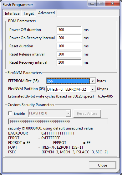
Tab 3 - Advanced
BDM Parameters
- Power Off duration
The length of time to turn off the power when having difficulty connecting to the target.
- Power On Recovery interval
The length of time to wait after powering on the target before attempting any operation.
- Reset duration
The length of time to apply the reset signal during a hardware reset.
- Reset Release interval
The length of time between releasing reset and releasing associated signals e.g. BKPT & BGND.
- Power Off Duration
The length of time to wait after resetting the target before attempting any operation.
FlexNVM Parameters
Some Coldfire+ and Kinetis devices support emulated EEPROM. This consists of a region of RAM and an associated backing store of EEPROM. The Flash controller transparently transfers data to-and-fro between the FlexRAM and the EEPROM backing store to provide emulation of a small-sector changeable EEPROM. The Flash controller uses a wear levelling mechanism to produce an emulated EEPROM with reasonable lifetime that is considerably longer that could be simply achieved using the large-sector (~1K) EEPROM available in these chips.
These controls allow the programming and initialisation of the EEEPROM in the target. The EEPROM created would then be used by a target program to preserve changing but persistent data. It is intended that this configuration would be only done once over a device lifetime as changing this configuration would probably invalidate the wear-levelling information maintained in the device. Changes during system development would not be an issue as the number of EEEPROM writes would be unlikely to be a significant portion of those of a deployed system.
- EEEPROM Size
This determines the size of the Emulated EEPROM located in the FlexRAM.
Selecting Unchanged/None with the mass erase programming option will disable the EEPROM.
Use with any other programming option e.g. Selective erase will leave the EEPROM setting of the device unchanged.
The latter is a useful combination that allows the general flash to be erased and re-programmed without affecting the EEEPROM data.
- FlexNVM Partition
This controls how much of the FlexNVM region is devoted to the EEPROM emulation. The remaining area may be used as conventional flash.
The ratio between the backing EEPROM size and the EEEPROM size greatly affects the effective lifetime of the EEEPROM.
- Estimated EEEPROM lifetime.
This provides an estimate of the lifetime of the EEEPROM i.e. the expected number of 16/32-bit write cycles to the EEEPROM before the reliability degrades too much. Please refer to the target data sheets & reference manuals for details of how this was calculated.
Note that the use of 8-bit writes to the EEEPROM will halve the effective lifetime.
|
|
Note: The programmer supports programming of the region of FlexNVM used as conventional Flash. It cannot program the emulated EEPROM.
Note: The programmer can only program this setting if the associated Flash IFR region is blank (unprogrammed). The only mechanism for erasing the IFR is a device mass-erase. Unless you know the device is unprogrammed, it is usual to use this setting with the mass-erase option.
|
Custom Security Parameters
This section allows the security area of the target to be programmed to a custom value.
- Enable - Enable the use of a custom value.
If this option is selected then the Security options on the Target tab are disabled and security is controlled by the information on this page.
If not selected then the Custom parameters will be disable and the information on this page will simply describe the security option selected on the Target tab.
- Flash area selector
This allows selection of the Flash area being customized. There is usually only a single security area so only a single option will be available. Devices with multiple Flash areas with individual security e.g. MCF51EM256 will have multiple regions selectable.
- Reset Values
This will reset all customized values to the default unsecured value.
- Custom value entry field
This allows entering the custom value to be used. The value will be padded with zeroes on the right to the required security area size.
- Information area
This area shows the security memory address and an abbreviated description of composition of the security value.
|
License
   USBDM Flash programmer & Utilties
   Copyright (C) 2009-2022  Peter O'Donoghue

   This program is free software; you can redistribute it and/or modify
   it under the terms of the GNU General Public License as published by
   the Free Software Foundation; either version 2 of the License, or
   (at your option) any later version.

   This program is distributed in the hope that it will be useful,
   but WITHOUT ANY WARRANTY; without even the implied warranty of
   MERCHANTABILITY or FITNESS FOR A PARTICULAR PURPOSE.  See the
   GNU General Public License for more details.

   You should have received a copy of the GNU General Public License
   along with this program; if not, write to the Free Software
   Foundation, Inc., 59 Temple Place, Suite 330, Boston, MA  02111-1307  USA
.png)
Truncated.png)